- Printing Industry
- Case Study: Boshsek’s Visual Inspection Solutions for Printed Circuit Boards(PCB)

In printed circuit board (PCB) manufacturing, the precision and stability of the inspection process directly determine the final product quality. The new-generation EOI-G Series and P Series appearance inspection solutions independently developed by Boshsek have been deployed on PCB production lines of electronics manufacturers. They deliver efficient and reliable detection solutions for long-standing industry pain points, including inner hole wall defects, foreign matter under solder mask, oil pooling and other common flaws.
01
Case Background
This electronics firm specializes in the R&D and manufacturing of high-precision, high-density and high-quality printed circuit boards (PCBs). Its products are widely applied in AI servers, computing networks, communications, automotive electronics and other sectors. The company boasts an annual total capacity of approximately 2 million square meters with consistently full capacity utilization.
02
Pain Points
Conventional AVI inspection systems have prominent limitations: high escape rates for hole wall defects, unstable detection performance on solder mask defects, and poor capability to spot micro foreign contaminants like fiber filaments. Furthermore, they cannot strike a balance between inspection throughput and detection accuracy, leading to frequent escapes and false calls.
03
Boshsek Precision Inspection Solutions
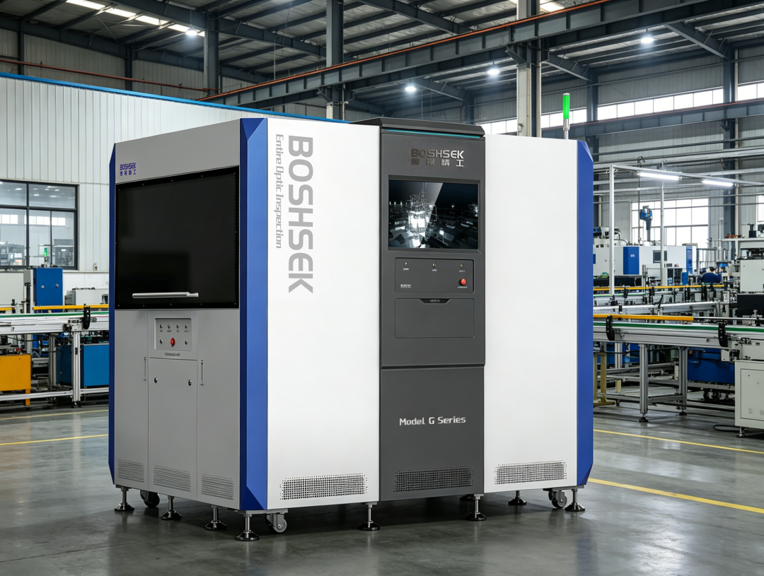
To address the above challenges, Boshsek provides customers with its self-developed new-generation appearance inspection machines: the EOI-G Series and P Series.
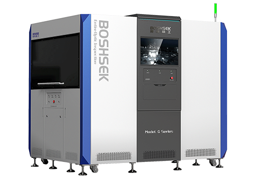
G Series:
Applicable Fields: Automotive electronics, mobile phones, AI computing cards and other industries
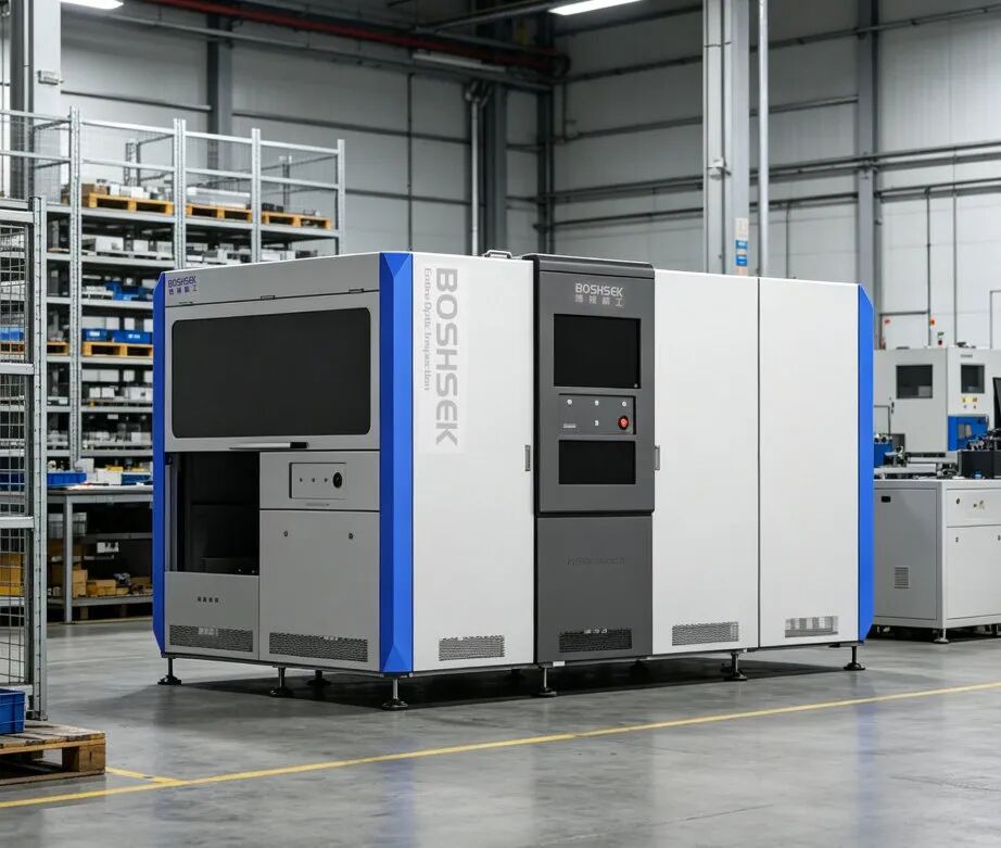
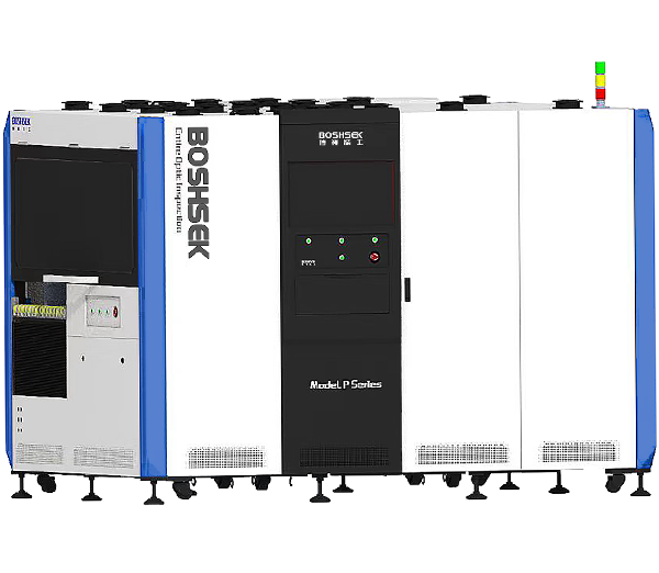
P Series:
Applicable Fields: Industrial control, servers and other sectors
01
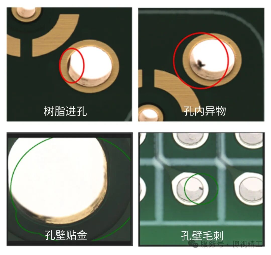
Hole Inner Wall Defect Metrology
This dual-light imaging technology combining red and white light was first proposed and industrialized by Boshsek. The two light sources complement each other, delivering a 95% inspection coverage rate for hole interiors. It effectively eliminates blind zones inside holes that plague conventional AVI systems and drastically boosts the inspection performance of hole wall defects for the electronics manufacturer.
02
NIR Independent Imaging & Metrology
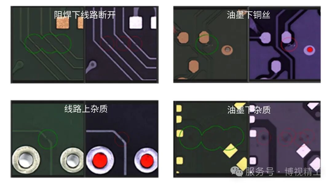
Boshsek is a pioneer in adopting NIR infrared penetration technology. Near-infrared light can penetrate deep into solder mask layers, enabling the electronics manufacturer to rapidly and clearly identify hidden defects under ink, including foreign contaminants on circuits, open circuits beneath solder mask, and copper filaments trapped under ink. This eliminates severe escape issues plaguing conventional AVI equipment, which lacks the capability to penetrate solder mask.
03
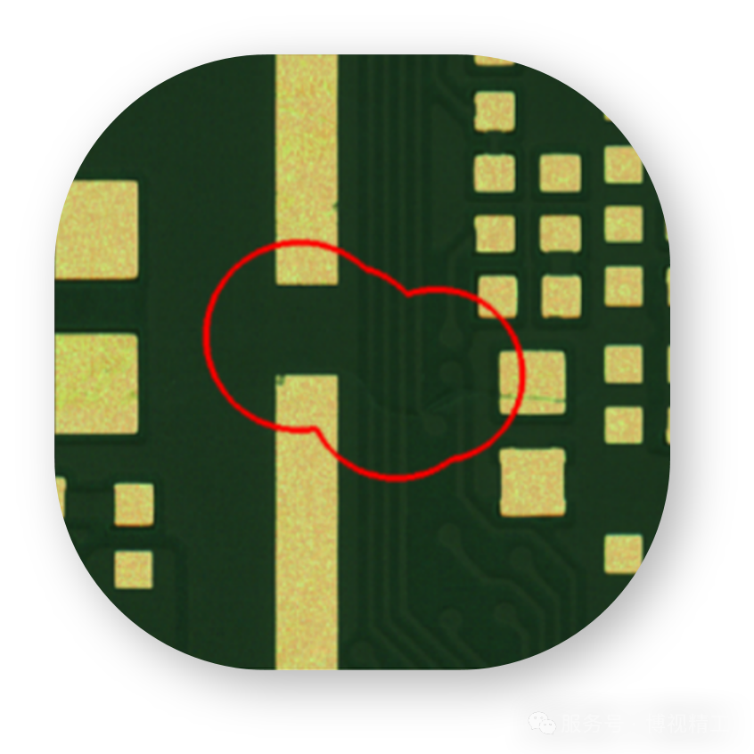
Non-metallic Solder Mask Foreign Material & Fiber Debris Inspection (COI)
This technology represents our company’s latest R&D achievement. It captures images from three distinct angles and integrates COI fused overlay images, RGB imaging and NIR imaging. The system is capable of detecting surface defects on circuit boards, as well as metallic and non-metallic defects hidden under solder mask, drastically cutting customers’ risks of missed detections for such flaws.
RGB Imaging
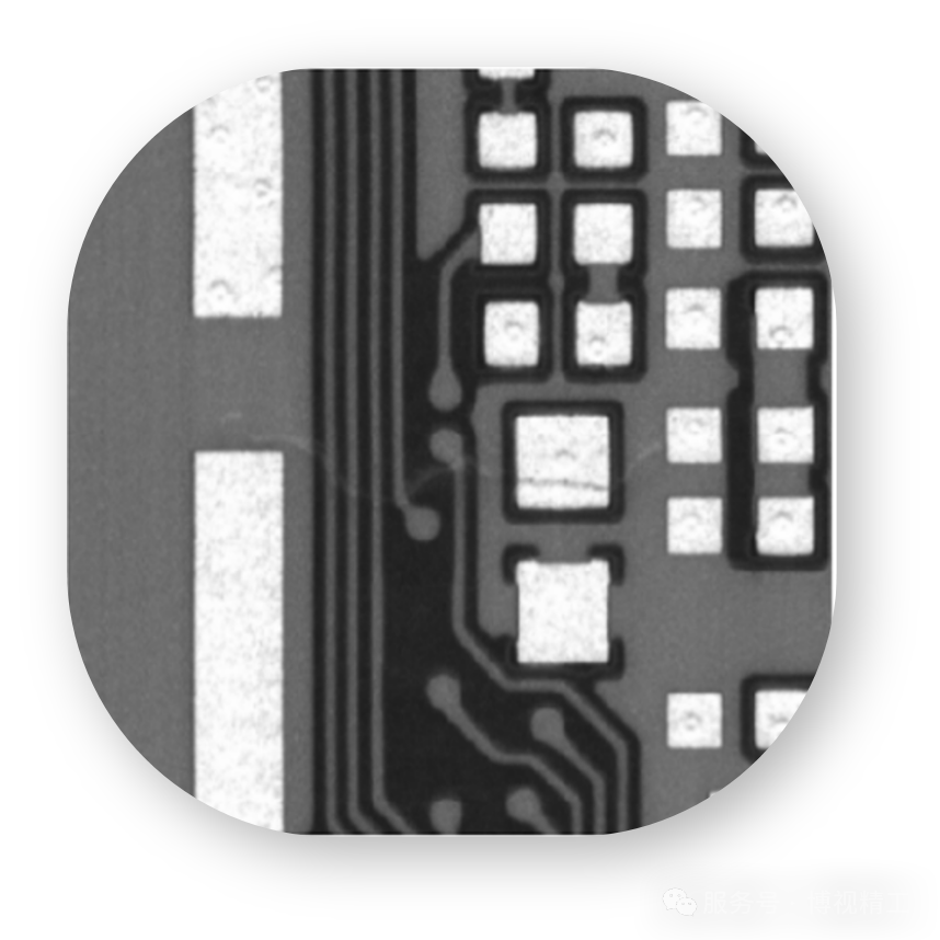
PCB Surface Defect Inspection
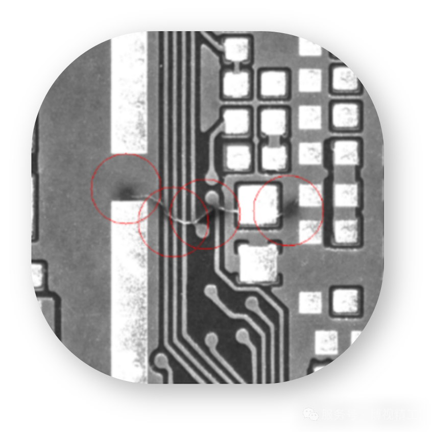
NIR Imaging
Detection of Metallic Defects Under PCB Solder Mask
COI Imaging
Detection of Non-Metallic Foreign Defects Inside PCB Solder Mask
04
EOI & AI Dual Computing Engine Service
Fast inspection speed, high defect capture rate and low false call rate, with zero data latency for AI post-processing.
05
Self-developed Brand-New AI 4.0 Intelligent System
Inspection throughput is doubled, perfectly matching high-speed production lines to cut costs and boost overall efficiency.
04
Application Performance
At present, the G&P series solutions have been operating stably on the electronics manufacturer’s production lines, greatly improving the coverage and accuracy of PCB inspection. Especially for high-precision manufacturing scenarios including automotive electronics, smart phones and servers, our solutions are highly compatible with the company’s product roadmap, providing reliable quality assurance for its further expansion into the high-end market.
Critical anomalies including hole interior foreign debris, solder mask pooling, non-metallic solder mask inclusions and fiber filaments often slip through inspection undetected. This consequently impairs the electrical performance and long-term service reliability of finished PCBs.
Inspection Size Range: 50×100 mm ~ 350×500 mm
Max Inspection Throughput:
1,000 PNL/H for single-sided boards
2,000 PNL/H for double-sided boards
Inspection Dimension Range: 50×140 mm ~ 620×820 mm
Maximum Inspection Throughput:
1,000 PNL/H (Single-sided PCB)
2,000 PNL/H (Double-sided PCB)


 (0512)57207966
 Phone number: (86) 180 1566 0849
 Email: sales@boshsek.com